 檢測認證人脈交流通訊錄
大連n型碳化硅_大連n型碳化硅襯底_沈陽n型碳化硅_豪麥瑞供_蘇州豪麥瑞材料科技有限公司專業從事氧化鋁球,氧化鋯球,陶瓷精加工,紡織陶瓷拋光加工業務.聯系電話:18962527682 網址:www.homraymaterial.cn
碳化硅半導體是新一代寬禁帶半導體,它具有熱導率高,與GaN晶格失配小等優勢,非常適合用作發光二極管,大功率電力電子材料。
采用碳化硅作襯底的LED器件亮度更高、能耗更低、壽命更長、單位芯片面積更小,且在大功率LED方面具有非常大的優勢。此外,碳化硅除了用作LED襯底,它還可以制造高耐壓、大功率電力電子器件如肖特基二極管(SBD/JBS)、絕緣柵雙極型晶體管(IGBT),晶閘管(GTO)、金屬氧化物半導體場效應晶體管(MOSFET)等,用于智能電網、太陽能并網、電動汽車等行業。
從整體上看,碳化硅半導體完整產業鏈包括:碳化硅原料-晶錠-襯底-外延-芯片-器件-模塊。
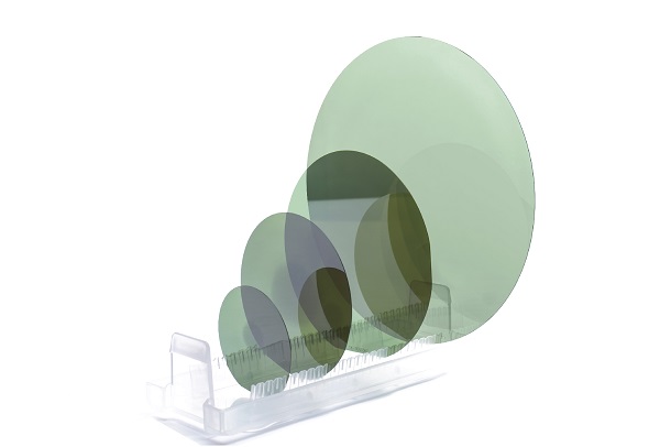
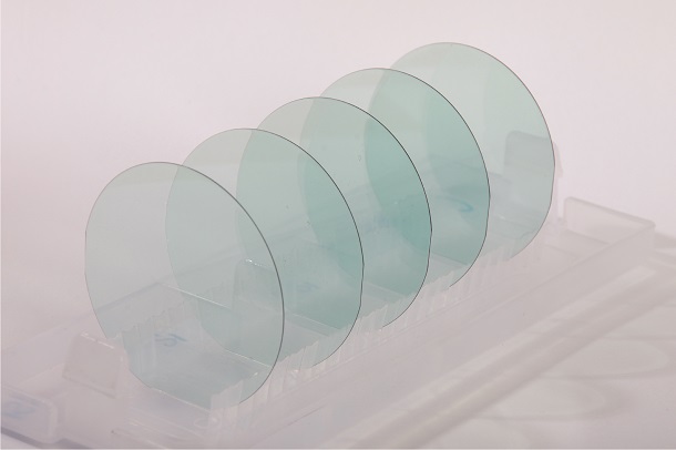
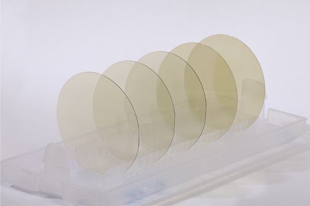
我們公司進口碳化硅晶圓,為我們的客戶提供所需的材料,讓客戶在這樣行業里促進技術的快速擴展。
產品介紹:
n-type SiC Substrate
PRODUCT DESCRIPTIONS
The Materials Business Unit produces a wide assortment of n-type conductive SiC products ranging in wafer diameters up to 150mm. This material is manufactured upon a high-volume platform process that provides our customers the highest degree of material quality, supply assurance and economies of scale.
Part Number
Description
W4NRF0X-0200
4H-SiC, n-type, Research Grade, 100mm, On-Axis, 0.013-2.0 ohm-cm, Standard MPD, 500um Thick, DoubleSided Polish Si Face CMP Epi Ready, Bare Substrate
W4NRF4C-U200
4H-SiC, n-type, Research Grade, 100mm, 4° Off-Axis, 0.015-0.028 ohm-cm, Ultra Low MPD ≤1/cm2, 350um Thick, Double-Sided Polish Si Face CMP Epi Ready, Bare Substrate
W4NPF4C-U200
4H-SiC, n-type, Production Grade, 100mm, 4° Off-Axis, 0.015-0.028 ohm-cm, Ultra Low MPD ≤1/cm2, 350um Thick, Double-Sided Polish Si Face CMP Epi Ready, Bare Substrate
W4NRF4C-B200
4H-SiC, n-type, Research Grade, 100mm, 4° Off-Axis, 0.015-0.028 ohm-cm, Ultra Low MPD ≤1/cm2, Low BPD ≤1500/cm2, 350um Thick, Double Sided Polish Si Face CMP Epi Ready, Bare Substrate
W4NPF4C-B200
4H-SiC, n-type, Production Grade, 100mm, 4° Off-Axis, 0.015-0.028 ohm-cm, Ultra Low MPD ≤1/cm2, Low BPD ≤1500/cm2, 350um Thick, Double-Sided Polish Si Face CMP Epi Ready, Bare Substrate
W4NRG4C-C1-V200
4H-SiC, n-type, Research Grade, 150mm, 4° Off-Axis, 0.015-0.028 ohm-cm, Very Low MPD ≤5/cm2, 350um Thick w/ 47.5mm Flat, Double-Sided Polish Si Face CMP Epi Ready, Bare Substrate
W4NPG4C-C1-V200
4H-SiC, n-type, Production Grade, 150mm, 4° Off-Axis, 0.015-0.028 ohm-cm, Very Low MPD ≤5/cm2, 350um Thick w/ 47.5mm Flat, Double-Sided Polish Si Face CMP Epi Ready, Bare Substrate
W4NRG4C-C1-U200
4H-SiC, n-type, Research Grade, 150mm, 4° Off-Axis, 0.015-0.028 ohm-cm, Ultra Low MPD ≤1/cm2, 350um Thick w/ 47.5mm Flat, Double-Sided Polish Si Face CMP Epi Ready, Bare Substrate
W4NPG4C-C1-U200
4H-SiC, n-type, Production Grade, 150mm, 4° Off-Axis, 0.015-0.028 ohm-cm, Ultra Low MPD ≤1/cm2, 350um Thick w/ 47.5mm Flat, Double-Sided Polish Si Face CMP Epi Ready, Bare Substrate
*C-faced polished wafers and 150mm LBPD substrates available upon request, lead times dependent on volume and requirements
FLAT LENGTH
Linear dimension of the flat measured with ANSI-certified digital calipers on a sample of one wafer per ingot
PRIMARY FLAT
The flat of the longest length on the wafer, oriented such that the chord is parallel with a specified low-index crystal plane.
PRIMARY FLAT ORIENTATION
The primary flat is the {1010} plane with the flat face parallel to the <1120> direction. Measured with Laue back reflection technique.
SECONDARY FLAT
A flat of shorter length than the primary flat, whose position with respect to the primary flat identifies the face of the wafer. Not applicable to 150mm wafers.
SECONDARY FLAT ORIENTATION
The secondary flat is the {11-20} plane with the flat face parallel to the <1010> direction. Measured with Laue back reflection technique.

MARKING
For silicon-face polished material, the carbon face of each individual wafer is laser-marked with OCR-compatible font, similar to definitions and characteristics in SEMI M12. For carbonface-polished material, the silicon face of each individual wafer is laser-marked.
PRODUCT SPECIFICATIONS
100mm Diameter n-type Substrates
Diameter
100.0 mm +0.0/-0.5 mm
Thickness
On-axis
500 μm ± 25 μm
Off-axis
350.0 μm ± 25.0 μm
Dopant
Nitrogen
Primary flat length
32.5 mm ± 2.0 mm
Secondary flat length
18.0 mm ± 2.0 mm
Surface orientation
On-axis
{0001} ± 0.25?
Off-axis
4.0? toward <1120> ± 0.5?
Surface finish
Back face optical polish, epi-face CMP
Orthogonal misorientation
± 5.0?
Primary flat orientation
<1120> ± 5.0?
Secondary flat orientation
90.0? CW from primary ± 5.0?, silicon face up
TTV
≤15 microns, full substrate
Warp
≤45 microns, full substrate
LTV (average, 1 cm2 site)
≤4 microns, full substrate
Edge chips by diffuse lighting
Production-grade
none permitted ≥0.5mm width and depth
Research-grade
qty. 2 ≥1.0 mm width and depth
150mm Diameter n-type Substrates
Diameter
150.0 mm ± 0.25 mm
Thickness
C1 specification
350 μm ± 25 μm
Dopant
Nitrogen
Primary flat length
47.5 mm ± 1.5 mm
Secondary flat length
None
Surface orientation
4.0? toward <11-20> ± 0.5?
Surface finish
Back face optical polish, epi-face CMP
Orthogonal misorientation
± 5.0?
Primary flat orientation
<11-20> ± 5?
Secondary flat orientation
N/A
TTV
≤10 μm
Warp
Production-grade
≤40 μm
Research-grade
≤60 μm
LTV (average, 1 cm2 site)
Production-grade
≤2 μm
Research-grade
≤4 μm
Edge chips by diffuse lighting
Production-grade
none permitted ≥0.5mm width and depth
Research-grade
qty. 2 ≥1.0 mm width and depth


蘇州豪麥瑞材料科技有限公司簡介:蘇州豪麥瑞材料科技有限公司是一家專業從事氧化鋁、氧化鋯產品、開發 制造、銷售于一體的企業,企業有國內前列的工藝,專業的技術人員,先進的生產設備和檢測手段。我公司生產的產品主要有:工業用各類氧化鋁粉包括(藍寶石長晶用粉,拋光用粉,拋光液用氧化鋁粉,片狀氧化鋁粉……),研磨用氧化鋁球,研磨用氧化鋯球,氧化鋁陶瓷件,精密氧化鋁陶瓷,專業陶瓷精加工服務,紡織陶瓷拋光精加工服務。
我公司產品齊全,被大范圍用于研磨、半導體、化工、拋光、制造、紡織等行業。由于我們的產品性能優良,久經耐用,深受廣大用戶好評。我們將優質的產品與服務奉獻客戶, 盡我們比較大的努力達到客戶的滿意。我們希望建立長期的友好合作關系,歡迎廣大國內外新老客戶來電咨詢及來廠考察洽談!蘇州豪麥瑞材料科技有限公司聯系方式:
王經理:18962527682
孫經理:18626214311
聯系電話:0512-65030678
網址:www.homraymaterial.cn
地址:蘇州市工業園區唯華路3號君地商務廣場5棟602室
-

檢測通手機版 
檢測通官方微信
檢測通QQ群


